How a CPU works
Modern CPUs are compicated beasts; however, the fundamental principles outlined in this article still hold true for them. Here is how they work.
If you want to know more about building a CPU from scratch, check out my project of a RRISC CPU or the accompanying presentation (PDF version) of a talk I gave about it.
CPU basics
The acronym CPU stands for “central processing unit” which rather precisely describes its function in a computer system. As the core of a computer, it does all the real work: Its task is to fetch instructions of a program from memory and execute them.
CPU instructions are rather primitive and coded in machine code, a numerical representation of those simple instructions. It usually takes many of them to do anything meaningful.
Since machine code is hard to work with for humans, a mnemonic representation, called assembly language, is used for writing low level software. Assembly language, as machine code, is always tied to a very specific CPU architecture, often called Instruction Set Architecture (ISA).
Without going into specifics, below is a comparison between human-friendly, symbolic assembly language (lda #$ca) and machine code (0a ca 00):
LDA #$CA     ; load register A with hexadecimal value CA

; machine code (hexadecimal): 0a ca 00
In the rest of this article, we’ll use the very simple RISC CPU as an example to illustrate the concepts discussed.
The example RRISC CPU
The main essential building blocks of a CPU are:
| Component | Purpose |
|---|---|
| Control Unit | does all the real work |
| One or more registers | store values to operate on |
Real CPUs consist of more building blocks, most notably an arithmetic logical unit (ALU) for simple integer arithmetic and bitwise logical operations, or a floating point unit (FPU) for performing floating point arithmetics.
Now, if this feels cyclic or like cheating to you, defining a component that does all the work inside the description of the component that is supposed to do all the work, further down the road, this will be resolved.
So the way a CPU operates, simply speaking, is to load instructions and values from memory into registers, operate on them and then store the result into memory or react to the result of the operation by jumping to a different part of the program.
In fact, that’s almost all the RRISC CPU ever does. In case you’re wondering, RRISC stands for Radically Reduced Instruction Set Computer, leaning on the acronym for the well established family of RISC architectures, Reduced Instruction Set Computers - but that’s a tangent for a seperate article.
With the above, we have introduced a few more relevant components:
Memory and Program Counter
| Component | Inside CPU? | Purpose |
|---|---|---|
| memory | no | stores program and data |
| instruction registers | yes | hold the current instruction and associated data |
| program counter | yes | points to memory location of next instruction |
First, there is memory: this is where the program and associated data resides. It is where the CPU reads instructions from and where instructions can make the CPU load operands from and store results to.
But the CPU needs to know where to load instructions from, more specifically, their memory location, referred to as the address. For that reason, the CPU contains a special counting register, the so-called program counter (PC), sometimes also called instruction pointer (IP). Every time the CPU fetches an instruction, it uses the PC to provide the address. For instructions consisting of multiple parts (bytes in our case), the CPU increments the PC in between fetches. More on that later.
The following illustration depicts a block diagram of our CPU (don’t worry about the details): 
As you can see, the RRISC CPU sports 7 registers.
An a bit more generic illustration can be found on Wikipedia:
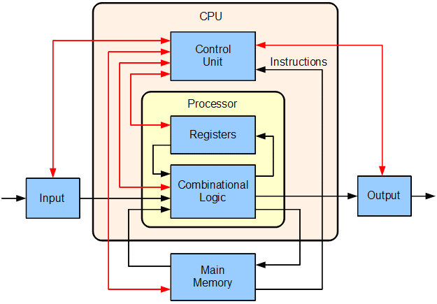
Note that in the illustration above, there is no notion of a program counter, it’s probably meant to be one of the registers. Also, some combinatorial logic is seen as not being part of the control unit.
Instruction Registers
When a CPU fetches instructions and operands, where does it store them? In the instruction registers. Our CPU has 3 instruction registers, which we consider to be part of the control unit:
| instruction register | purpose |
|---|---|
| instruction register 1 | holds the opcode of the instruction |
| instruction register 2 | holds the first part of the operand (LOW byte) |
| instruction register 3 | holds the second part of the operand (HIGH byte) |
The opcode is the actual machine code of the instruction, just a number. For the sake of simplicity, all instructions of the RRISC CPU are 3 bytes wide. That means that an instruction always consists of all 3 bytes for the 3 instruction registers, no matter if the operation needs an operand or not.
The concept of HIGH byte and LOW byte
A byte consists of 8 bits, each of which can take a value of either 0 or 1. 8 bits together can be interpreted as a binary number. 8-bit numbers (bytes) give us a permutation of 256 different values ranging from 00000000 to 11111111 in binary notation, which correspond to the decimal values ranging from 0 to 255.
Sometimes, however, 8 bits are not enough. Consider the memory for example. If we want to load a value from memory, we have to provide an address (location in memory). It would be a shame if we could only access 256 different addresses in memory. Most of our programs will be larger than that.
So, to address more memory, we simply add a second byte. With two bytes combined, we can have 16-bit binary numbers, ranging from 0 to 65535. We call the upper, leftmost, half of the 16-bit number the HIGH byte and the lower, rightmost half the LOW byte.
Without digging deeply into binary arithmetic, the formula to calculate the value from a value split into low and high bytes, is:
value = HIGH_byte * 256 + LOW_byte
With the basics out of the way, we can now move on to how the control unit works.
From Combinatorial Logic to Control Unit
To understand how a control unit works, we have to start with the basics.
Combinatorial Logic
We start with combinatorial logic circuits. A combinatorial logic circuit, in digital electronics, is a very basic digital logic circuit (only 0s and 1s) whose output only depends on its inputs.
As such, they can be seen as implementing a pure function (inputs –> output). Since all inputs and the output are digital and can only have discrete values, the entire function can be described with a function table, listing the desired output for all possible combinations of the input.
Example:
| Input A | Input B | Output X |
|---|---|---|
| 0 | 0 | 1 |
| 0 | 1 | 0 |
| 1 | 0 | 0 |
| 1 | 1 | 1 |
Combinatorial logic circuits are built from fundamental components, the so-called logic gates. A logic gate is a little electronic circuit that implements a boolean function. Without going into details, fundamental logic gates to describe any function table are:
- AND: output is 1 if all inputs are 1, else 0
- OR: output is 1 if any input is 1, else 0
- NOT: output is 1 if input is 0, else 0
The clue about logic gates is that they are easily translated into physical form by implementing them using transistors.
So, our function table above can be described using boolean algebra directly translating to logic gates like this:
X = ( {NOT A} AND {NOT B} ) OR (A AND B)
Above function can also be depicted in schematic form using logic gates: 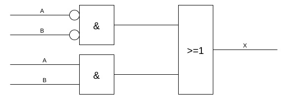
Cunningly, AND gates are depicted containing an & symbol and OR gates contain >=1. The little circles at the A and B inputs of the top left AND gate are shorthand notation for NOT, saving us from drawing two NOT gates, which are more common-sensically called inverters.
One critical observation can be made about combinatorial logic circuits: they are stateless or asynchronous, meaning, any change of the inputs is reflected at the output immediately. Without a concept of timing, how shall our control unit ever execute one step at a time?
Introducing State
It is time to introduce the concept of state to our growing control unit.
We achieve that by introducing a so-called D-Flipflop at the output of our circuit. A D-flipflop can be seen as a 1-bit memory and can be built using basic logic gates.
It works like this:
- when a CLOCK signal arrives (rising edge):
- its output is set to the value of its input
- the output does not change anymore, even if the input changes
- this state is kept until the next CLOCK signal arrives
With rising edge we mean the CLOCK signal changing from 0 to 1.
So, when we add the D-flipflop, we get time-dependent, stateful or synchronous behavior:
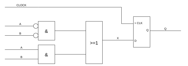
Let’s examine our new circuit and look at a timing diagram:

- In the beginning, A is 0, B is 0, CLOCK is 0. Output Q is also 0.
- A little later, B becomes 1 but nothing else changes. The flipflop keeps its state and Q remains 0.
- Next, indicated by the first red dotted line, CLOCK changes from 0 to 1. A rising edge! So this time, the D-flipflop captures the result of the combinatorial logic. According to the function table, X(0, 1)=0, so Q remains 0.
- Q goes down to 0 and shortly afterwards A becomes 1. Now we have A=1 and B=1, so our combinatorial logic outputs a 1 - but since the D-flipflop is not triggered yet, Q remains 0.
- However, next we see a rising edge at the CLOCK signal! Now the output of the combinatorial logic (A=1, B=1 –> X=1) is captured by the D-flipflop and the output Q changes from 0 to 1.
- … I leave the rest as an excercise for the reader
Great, now we are on step further: our circuit only reacts to input when it sees a clock signal. It has state. But how can we make it go from one step to the next?
Finite State Machines
In order to achieve that, we feed back the state output into the inputs of the combinatorial logic. By doing that, we create a so-called Finite State Machine (FSM).
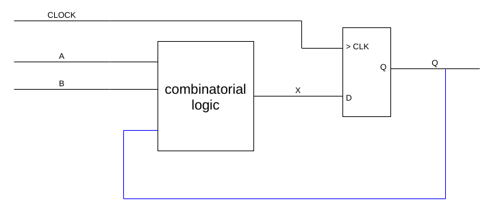
Now our output (at rising clock edge) is dependent on both:
- the inputs
- the current state
We could also say that the next state Q depends on:
- the condition (inputs A, B)
- the current state
Which means, we can jump from state to state given certain conditions, expressed by the inputs.
Consider the following function table of the combinatorial logic:

With every clock signal, the circuit can now change its state but it only does so when certain conditions are met.
In the illustration below, the state transition conditions are marked in blue:

And with that we can design complex state machines that execute one step at a time and react to inputs, such as instruction opcodes.
Control Unit
It is common practice though, when designing a control unit, to separate concerns a bit:
- we use a finite state machine to define the state of the CPU
- we then use an additional combinatorial logic to decode both CPU state and input signals into the output signals

This makes for a cleaner design that is more easy to maintain.
The RRISC Control Unit
With all that knowledge under our belt we have a basic understanding that a Control Unit can be built from a state machine and combinatorial logic. But what should the control unit do? What states should it have?
So, back to the example of the RRISC CPU, the control unit knows the following states that it executes in order:
| state | function |
|---|---|
| wakeup | only ever present immediately after a reset, sets everything up so that an instruction can be fetched |
| ram_wait_1 | a wait state giving the RAM (memory) time to output the instruction of the program counter |
| fetch_1 | the RAM’s output is loaded into intruction register 1 and the program counter is incremented by one |
| ram_wait_2 | wait state for the RAM |
| fetch_2 | the first operand byte is loaded into instruction register 2 and the program counter is incremented |
| ram_wait_3 | wait state for the RAM |
| fetch_3 | the second operand byte is loaded into instruction register 3 |
| decode | preparing for a potential load/store operation, the RAM address is set to operand HIGH and LOW bytes |
| execute | depending on opcode, load/store + PC increment or jump = PC load is performed |
The next state after execute is ram_wait_1 again.
When you consider that all CPU registers are D-flipflops, just with 8 inputs and outputs each instead of the 1-bit variants we saw before, and that the RAM also behaves a bit like a D-flipflop, you can see how easy writing to registers is: you just have to “clock” the right one.
Executing a RRISC instruction
Let’s look more deeply into what happens when we execute an instruction:
lda # $CA ; load register A with immediate value 0xCA
The instruction lda # $CA does the following:
- it takes the value $CA (202 in hexadecimal)
- it stores this value in register A
The image below shows the CPU going out of reset (wakeup) and then executing the instruction in 8 clock cycles.
The thin red vertical line to the right in the image is placed at ca. 90 nanoseconds, right after the execute phase of the instruction. In the last, blue line of the diagram you can see cpureg_a (register A) receiving the value CA at the end of execute.
If you look carefully, you can see that value travel from ram_out (the output of the RAM) via debug_inr2 (instruction register 2 containing the operand, the value CA in our case) to register A.

| time | clock cycle | description |
|---|---|---|
| 0 .. 10ns | - | - ram_addr is reset to 0, so execution will start from there - the cpu is prepared to start with state wakeup - the RAM is in reset mode, too, outputting zeros |
| 10 .. 15ns | 0 | - cpu is active in wakeup, doing nothing until the next clock cycle |
| 15 .. 25ns | 1 | - cpu enters ram_wait_1 state, giving the RAM time to output the opcode - cpu is active in wakeup, doing nothing until the next clock cycle - ram outputs the opcode at address 0, ready for the cpu to grab it in the next cycle |
| 25 .. 35ns | 2 | - now in fetch_1, the cpu loads ram_out into instruction register 1, shown as debug_inr1 - it also sets pc_clock to 1, so the program counter will be incremented in the next cycle - program counter increments ram_addr to 1 |
| 35 .. 45ns | 3 | - cpu in ram_wait_2 - ram output is valid at the end of the cycle: $CA |
| 45 .. 55ns | 4 | - now in fetch_2, the cpu loads ram_out into instruction register 2, shown as debug_inr2 - it also sets pc_clock to 1, so the program counter will be incremented in the next cycle - program counter increments ram_addr to 2 |
| 55 .. 65ns | 5 | - cpu in ram_wait_3 - ram output is valid at the end of the cycle: $00 |
| 65 .. 75ns | 6 | - now in fetch_3, the cpu loads ram_out into instruction register 3, shown as debug_inr3 - (no program counter increment here) |
| 75 .. 85ns | 7 | - cpu enters decode stage - it proactively disconnects ram_addr from the program counter and sets it to instruction registers 3 (00) and 2 (0A), just in case a ram load / store or jump operation is executed - hence, ram_addr changes to 0a - now the ram would have time to output the contents of address 0a in case it’s needed |
| 85 .. 95ns | 8 | - in execute, the contents of instruction register 1 are loaded into register A - note: register A captures the value at the beginning of the next cycle - since it is not a jump instruction, pc_clock is raised again to increment the program counter to 3, where the next instruction will start - ram_addr is switched back to the program counter |
| 95 .. 100ns | 9 | - the cpu goes into ram_wait_1 again, to give the ram time to output the next instruction |
And voila! This is how a CPU works! That’s all there is to it! Well, by example of a super simplified CPU.
Please note:
Some concepts in this article have been simplified or reduced to their core. Many details have been omitted like going into binary, decimal and hexadecimal number systems, just to name some. If you find this article inaccurate, lacking, or if you find errors, please let me know - dm me on twitter and I will fix it.
If you want to learn more, check out:
- the project webpage of my RRISC CPU
- the accompanying presentation (PDF version) of a talk I gave about it.
- the RRISC CPU on GitHub